
Overview Of The Semiconductor Capital Equipment Industry
Introduction
If you do not know anything about semiconductors and you listen to a presentation by a semiconductor capital equipment company, you will quickly be lost. I know because I was there before. Management continuously rattles off terms like logic, foundry, DRAM, NAND, fab, wafer, etc. I said to myself, “what are these guys talking about?!?!” Eventually, I had to do a deep dive into the industry to understand it which included reading an entire book about it.
The semiconductor industry manufacturers integrated circuits (“chips”) for a variety of electronics, including computing devices, network equipment, and storage devices. The rise of new technological advancements such as autonomous vehicles, big data analytics, edge computing, immersive devices (e.g.virtual reality), internet of things, machine learning, robotics, and so on are not only requiring more chips but continually more advanced chips. This is good business for companies who make the equipment to advance chip technology. Furthermore, China is investing aggressively in all these new technologies which is also increasing the demand for semiconductor equipment.
More Data = Semiconductor Growth Opportunity
The following presentation slide shows the broad opportunity set for the semiconductor industry in this new “Data” era:

source: KLA-Tencor NASDAQ 39th Investor Conference presentation; click to enlarge
This slide shows the expected revenue growth out to 2025 for the end markets of the semiconductor industry:
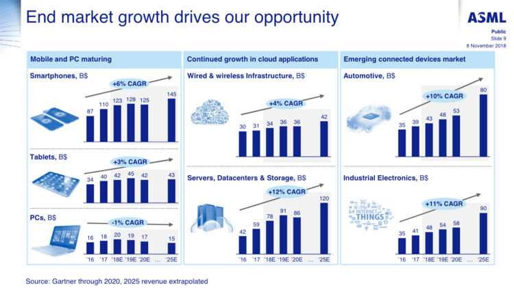
source: ASML presentation, Gartner; click to enlarge
You can see from this slide that the #1 growth driver for the semiconductor industry is Servers, Datacenters & Storage which is being driven by the rise of cloud computing.
These growth drivers are adding up and semiconductors are increasingly becoming a larger part of the world economy, as this slide shows:
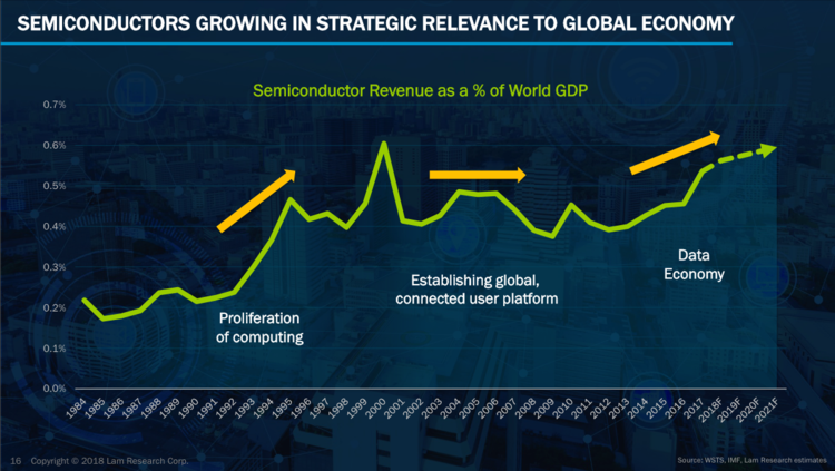
source: Lam Research investor presentation, WSTS, IMF; click to enlarge
Semiconductors are an important growth business and semiconductor capital equipment is an essential sub-industry worth understanding.
Chip Types
At a high level, there are two types of chips that are commonly produced by semiconductor manufacturers like Intel (INTC), Micron (MU), Samsung (SSNNF; SSNLF), SK Hynix (HXSCF; HXSCL), and Taiwan Semiconductor (TSM).These are memory and logic. Let's take a look at each of these.
Memory chips are used to store data electronically in the form of bits (8 bits = 1 byte). The most common types of memory chips made by the industry today are Dynamic Random Access Memory ("DRAM") and NAND flash. DRAM is volatile memory, which means it temporarily stores each bit of data in a separate capacitor while the associated device is powered on. DRAM is commonly used by data servers and mobile devices. NAND (short for NAND flash) is non-volatile memory ("NVM"), which means it stores data even if the power is switched off. It is called NAND because it is a type of memory that resembles the NAND (not-and) logic. NAND is commonly used in memory cards and solid state drives("SSD"). The major trend in memory today is the switch to three-dimensional (3D) memory where memory cells are built vertically, instead of horizontally (planar), which increases memory bit density.
Logic chips are the fundamental building blocks for digital electronics. Logic chips are constructed from connecting individual digital logic gates that perform logical operations of AND, OR and NOT on binary numbers.(This is where the NAND or not-and comes from). Logic chips perform calculations that drive computer processing.
Semiconductor manufacturers are generally focused on designing chips for various device applications. The semiconductor capital equipment industry (“semi-cap” for short) provides the equipment for these manufacturers.
The semiconductor industry is to electronics what the mining industry is to finished metal products. Taking this one step further, the semi-cap industry supplies the“picks and shovels” for the broader semiconductor industry.
Chip Manufacturing
Chips are constructed from wafers of silicon in the clean rooms of fabrication facilities (“fabs”).These wafer fabs are sometimes referred to as the “front end” of the production process. Fabs are very expensive to build because these clean rooms are something like 1,000 times cleaner than a regular room with constant air circulation so that no speck of dust gets on the wafers.
Here is how KLA-Tencor described the semiconductor fabrication process in their most recent annual report:
The semiconductor fabrication process begins with a bare silicon wafer—a round disk that is typically 200 millimeters or 300 millimeters in diameter, about as thick as a credit card and gray in color. The process of manufacturing wafers is in itself highly sophisticated, involving the creation of large ingots of silicon by pulling them out of a vat of molten silicon. The ingots are then sliced into wafers. Prime silicon wafers are then polished to a mirror finish. …
The manufacturing cycle of an IC is grouped into three phases: design, fabrication and testing. IC design involves the architectural layout of the circuit, as well as design verification and reticle generation. The fabrication of a chip is accomplished by depositing a series of film layers that act as conductors, semiconductors or insulators on bare wafers. The deposition of these film layers is interspersed with numerous other process steps that create circuit patterns, remove portions of the film layers, and perform other functions such as heat treatment, measurement and inspection. Most advanced chip designs require hundreds of individual steps, many of which are performed multiple times. Most chips consist of two main structures: the lower structure, typically consisting of transistors or capacitors which perform the “smart” functions of the chip; and the upper “interconnect”s tructure, typically consisting of circuitry which connects the components in the lower structure. When all of the layers on the wafer have been fabricated, each chip on the wafer is tested for functionality. The wafer is then cut into individual chips, and those chips that passed functional testing are packaged. Final testing is performed on all packaged chips.
There are three primary aspects to manufacturing chips at the front end. These are deposition, lithography, and etch and clean. All three of these aspects require process control. At a very high level, this is how it works:
-
Layers of insulating or conducting materials (chemicals) are sprayed or deposited onto a silicon wafer during deposition.The most commonly used deposition solutions used are (1) atomic layer deposition ("ALD"), (2) epitaxy, and (3) variations of vapor deposition.
-
Inside a Step-and-Scan system (or stepper), special lights (similar to lasers or x-rays) are shined through a photomask to transfer designs developed by engineers unto the wafer during lithography.
-
Some of the material on the wafer is etched away to create desired patterns during the etching and the unwanted materials are removed during the clean process.
These processes are repeated to create the chips on the wafers before elements are finally added to form transistors. Throughout these processes, process control equipment is used for inspection and metrology (measurement) to remove defects and increase yields (i.e., increase the number of usable chips).
Deposition, lithography, etch and clean, and process control are the primary component categories of wafer fabrication that the semi-cap companies specialize in making equipment for. Roughly 85% of the capital expenditures (CAPEX) made by chip manufacturers for semiconductor equipment goes towards wafer fabrication equipment (WFE).Thus, most of the semi-cap industry conversation revolves around the main producers of wafer fab equipment.
The WFE market is now primarily concentrated into the hands of just a few companies: Applied Materials (AMAT), ASML (ASML), KLA-Tencor (KLAC), Lam Research (LRCX), Tokyo Electron (TOELF; TOELY), Screen Semiconductor (DINRF; DINRY), and Hitachi High Tech (HICTF).
-
In deposition, Applied Materials has the leading share (~50%), followed by Lam Research and Tokyo Electron.
-
In lithography, ASML focuses on the high end and has a dominant share (~75%+), followed by Nikon (NINOF; NINOY) and Canon (CAJ). These three companies control almost the entire lithography market.
-
In etch, Lam Research has the leading share (~57%), followed by Tokyo Electron and Applied Materials.
-
In process control, KLA-Tencor is the dominant player (~55% share).
In 2017, WFE CAPEX crossed the $50 billion threshold for the first time, as shown on the left-hand side of the following slide:
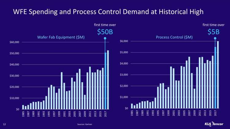
source: KLA-Tencor NASDAQ 39th Investor Conference presentation, Gartner; click to enlarge
The remaining 15% of the semi-cap industry CAPEX comprises the“back end” of chip production which includes testing wafers, cutting the wafers into chips, and packaging the chips. The primary 2 components of the back end where semi-cap companies also compete can best be described as test and packaging.
There are 3 categories of chip manufacturers that buy equipment: logic, memory, and foundry. Here is what each of these categories represents:
-
Logic represents companies manufacturing their own logic chips in their own factories.
-
Memory represents companies manufacturing their own memory chips in their own factories.
-
Foundries are companies with large fabs that produce multiple chips for multiple companies who do not want to manufacture their own. Taiwan Semiconductor Manufacturing Company is the largest foundry in the world.
Semi-cap companies reference these 3 types of customers in their financials and other investor materials.
Conclusion
I hope you found this overview of the semi-conductor capital equipment industry helpful. Semi-cap companies are the behind-the-scenes producers of the tools used to create the building blocks that underpin the new technologies of our modern era. They provide a unique outlet for investing in the technology sector.
Disclosure: KLA-Tencor is a holding in client portfolios. I have an economic interest in the performance of the stock. The above True Vine Letter is an excerpt from a recent more


Impressive stuff.
Harry,
Thanks for the kind word.
This is great. I've often asked "what are these guys talking about?!"
Barry,
I knew I wasn't the only one!
You aren't!