

Global wafer fab equipment spending is moving further into record territory. The latest projection of $135.2 billion for 2026 represents approximately 16.9% growth from the stated 2025 level of $115.7 billion. More important than the headline increase, however, is the changing composition of that spending.
The current expansion is no longer being driven primarily by a single category such as leading-edge foundry capacity. Memory, advanced logic, mature-node manufacturing, advanced packaging and supporting fab infrastructure are all contributing, although at substantially different rates.
The breadth of this investment cycle distinguishes it from the more concentrated expansion investors anticipated a year ago. At that time, the equipment thesis centered primarily on Taiwan Semiconductor Manufacturing Company (NYSE: TSM), advanced logic and the manufacturing requirements of AI accelerators. Those areas remain important, but the recovery in memory capital expenditures has added another major source of equipment demand.
The evidence is visible in capital-expenditure plans from Samsung Electronics (OTC: SSNLF), Micron Technology (NASDAQ: MU), SK Hynix and TSMC, as well as in the order books of semiconductor equipment suppliers. The resulting investment opportunity is attractive, but semiconductor equipment should not be treated as a single uniform category. Lithography, deposition, etch, process control and advanced packaging suppliers will participate differently, while China exposure creates materially different risk profiles.
Global WFE Spending Accelerates in 2026
According to Table 1, global WFE spending is projected to increase from $115.7 billion in 2025 to $135.2 billion in 2026, representing growth of approximately 16.9%. Within that total, 300mm DRAM equipment spending is projected to rise 29% to $37 billion, while 300mm 3D NAND equipment investment is expected to increase 28% to $14 billion.
The remaining logic, foundry and other WFE categories are projected to reach approximately $84.2 billion in 2026, up 10.6%. Memory therefore represents the fastest-growing major portion of the equipment market, even though logic, foundry and other applications continue to account for most industry spending.
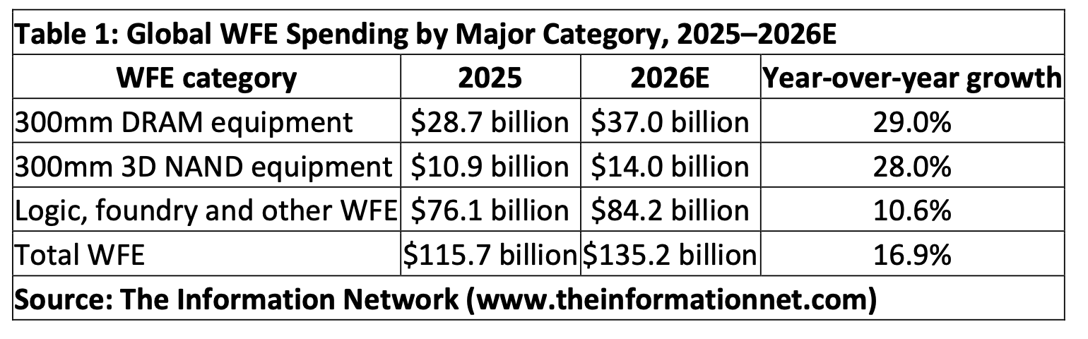
The 2025 DRAM and NAND amounts are calculated from the stated 2026 projections and growth rates. Logic, foundry and other WFE is the residual required to reconcile the memory forecasts with total WFE spending. Differences may result from rounding.
The table changes the interpretation of the current cycle. Logic and foundry remain the largest sources of equipment spending, but memory is providing the acceleration. This creates a broader demand environment than one supported almost entirely by TSMC’s leading-edge capital expenditures.
Memory Investment Broadens Beyond HBM
Samsung, Micron and SK Hynix are increasing capital expenditures simultaneously, although their spending priorities differ. All three are allocating more capital to advanced DRAM, HBM, NAND, cleanrooms and supporting infrastructure.
Samsung reported Q2 2026 capital expenditures of 16.8 trillion won, including 15.4 trillion won within its Device Solutions division. The spending is directed toward construction and infrastructure at Pyeongtaek, along with development of HBM4, DDR5 and SOCAMM2 products. Samsung had previously trailed SK Hynix in converting its memory strategy toward HBM, but its current spending indicates that it is attempting to narrow the competitive and production gap.
Micron raised its fiscal 2026 capital-expenditure estimate to approximately $27 billion and expects another significant increase in fiscal 2027. More than half of the incremental spending is expected to support plants and cleanroom construction, although production-equipment expenditures are also projected to increase year over year.
That distinction is important for equipment investors. Cleanroom construction expands Micron’s ability to install additional tools, but it does not translate immediately into an equivalent increase in productive wafer capacity or equipment revenue. Instead, it improves visibility into equipment demand extending beyond the current fiscal year.
SK Hynix’s 2026 capital expenditure is expected to reach the upper end of the 40 trillion won range. Its priorities include the M15X production ramp, construction of the first-phase cleanroom at Yongin, the P&T7 advanced-packaging facility and the M17 NAND production base. The dedicated packaging investment demonstrates how HBM capital intensity extends beyond front-end wafer fabrication into stacking, bonding, testing and thermal management.
According to Table 2, investment in 300mm DRAM and 3D NAND equipment is projected to reach a combined $51 billion in 2026. DRAM represents approximately 72.5% of the total, reflecting the manufacturing intensity of HBM and advanced DDR5 production.
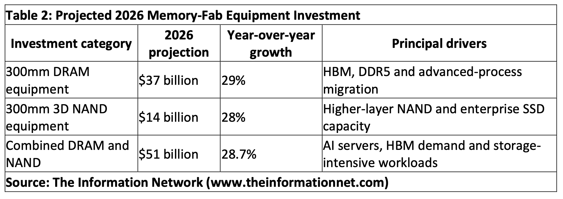
The similarity between the DRAM and NAND growth rates indicates that the memory recovery is broadening beyond HBM-related DRAM. Higher-layer NAND and enterprise SSD capacity are also contributing to equipment demand as AI data centers generate larger storage requirements.
Despite the sharp increase in capital expenditures, new memory supply is not expected to fully match projected demand. A significant portion of current spending is being directed toward facilities that will support later equipment installations. The time required to construct cleanrooms, install tools, qualify manufacturing processes and reach acceptable yields creates a substantial delay between capital authorization and commercial output.
This delay reduces the likelihood that the 2026 spending increase will immediately produce the oversupply historically associated with memory upcycles. It does not eliminate that risk, but it pushes the potential inflection further into the future.
Logic and Foundry Investment Remains Anchored by TSMC
Memory is providing the highest equipment growth rate, but TSMC remains the largest individual contributor to advanced logic and foundry investment. TSMC raised its 2026 capital-expenditure guidance from $52–56 billion to $60–64 billion while increasing its expected full-year dollar revenue growth to slightly above 40%.
Approximately 70% to 80% of TSMC’s budget is allocated to advanced process technologies, about 10% to specialty technologies and between 10% and 20% to advanced packaging, testing, mask manufacturing and related investments.
The packaging allocation reflects a structural change in AI processor manufacturing. Leading-edge logic dies increasingly must be integrated with multiple HBM stacks using interposers, substrates and high-density interconnects. As a result, advanced packaging is becoming a separate and increasingly important equipment market rather than merely the final stage of semiconductor assembly.
Below TSMC, foundry companies are expanding at a smaller scale. United Microelectronics Corporation (NYSE: UMC) raised its 2026 capital expenditure to approximately $2 billion, primarily for 12-inch wafer capacity. Semiconductor Manufacturing International Corporation’s planned investment is approximately $8 billion, while Hua Hong Semiconductor spent $920 million during Q1 2026. Hua Hong’s Fab9B is expected to complete construction during Q4 2026, followed by equipment installation and a production ramp during 2027.
Vanguard International Semiconductor plans to maintain capital expenditures of approximately NT$60–70 billion, primarily for construction of 12-inch production capacity. These projects indicate that mature and specialty process investment remains active even as AI accelerators and advanced logic dominate industry headlines.
According to Table 3, the major capital programs differ considerably in their timing and composition. Memory manufacturers are allocating significant amounts to cleanrooms and advanced packaging, while TSMC remains heavily concentrated on advanced processes. The remaining foundries are directing more of their budgets toward 12-inch mature and specialty capacity.
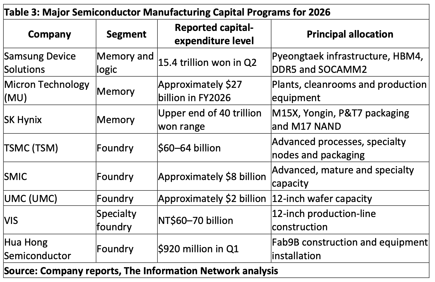
The table also demonstrates why semiconductor capital expenditures cannot be translated directly into equipment revenue on a dollar-for-dollar basis. Capital budgets include buildings, cleanrooms, utilities, land and packaging facilities in addition to semiconductor production tools. Equipment suppliers benefit as those facilities move toward tool installation, but the resulting revenue may occur several quarters after the initial capital commitment.
Equipment Orders Confirm the Expansion
Capital-expenditure guidance establishes customer intent, but equipment orders provide more direct evidence of near-term demand. ASML Holding (NASDAQ: ASML) ended Q4 2025 with net bookings of €13.2 billion and a total backlog of €38.8 billion. Its order base extends into 2027, providing unusually strong visibility for an industry that has historically been highly cyclical.
The importance of ASML’s order book extends beyond its absolute size. Memory orders exceeded logic orders during Q4 2025, demonstrating that the DRAM recovery had progressed from corporate guidance into equipment procurement. This supports the conclusion that the equipment cycle is broadening rather than merely extending the earlier TSMC-led expansion.
Applied Materials (NASDAQ: AMAT), Lam Research (NASDAQ: LRCX), KLA Corporation (NASDAQ: KLAC) and Tokyo Electron (OTC: TOELY) should also benefit, although their exposures differ.
Lam has substantial leverage to the memory recovery through its etch and deposition businesses, particularly as DRAM and NAND structures become more complex. Applied Materials participates across deposition, materials engineering, implant, process control and packaging-related applications. KLA benefits from increasing inspection and metrology intensity across advanced logic, memory and packaging.
ASML remains the cleanest structural participant because of its lithography position and the visibility provided by its backlog. Applied Materials and Lam Research may provide greater operational leverage to accelerating memory investment, but both face more uncertainty related to China and product-specific export restrictions.
China Represents a Separate Equipment Cycle
China’s semiconductor investment should be divided between leading-edge and mature-node manufacturing. Export controls limit Chinese access to the most advanced lithography and selected deposition, etch and related manufacturing technologies. These restrictions constrain the pace at which Chinese foundries can expand leading-edge production, regardless of the capital available.
The mature-node market is different. Chinese manufacturers continue to build capacity for automotive, industrial, power-management, display-driver and consumer-semiconductor applications. Much of this investment remains accessible to international equipment suppliers, although the scope of permitted shipments can change as export controls evolve.
China is also developing domestic equipment suppliers across deposition, etch, cleaning, thermal processing, ion implantation and process control. This creates a competitive threat extending beyond the immediate effects of export restrictions. International suppliers may continue generating substantial revenue in China while gradually losing share to domestic systems in individual equipment categories.
Investors must therefore consider two separate risks. The first is the possibility of additional restrictions on equipment shipments by international suppliers. The second is the longer-term substitution of imported tools by Chinese equipment. Companies with high China revenue concentration should be valued with both risks in mind, even when their non-China order books remain strong.
Investor Takeaway
I rate the semiconductor equipment supplier group a Buy based on the breadth, visibility and composition of the 2026 capital cycle. TSMC’s increased capital budget supports advanced logic and packaging, while the simultaneous investment increases from Samsung, Micron and SK Hynix strengthen the memory-equipment outlook. The projected 29% increase in DRAM equipment spending and 28% increase in 3D NAND equipment spending indicate that the expansion is no longer dependent on a single customer or semiconductor category.
ASML offers the clearest visibility because of its €38.8 billion backlog, lithography position and order coverage extending into 2027. Applied Materials and Lam Research provide greater leverage to the memory recovery through deposition and etch, while KLA benefits from increasing process-control intensity across advanced logic, memory and packaging. Investors should nevertheless distinguish between capital allocated to cleanroom construction and capital committed to production equipment because the timing of supplier revenue will differ.
The principal cyclical risk remains eventual memory overinvestment. Samsung, Micron and SK Hynix have historically continued adding capacity after demand growth began to moderate, producing oversupply and subsequent reductions in equipment spending. Current investment remains concentrated heavily on infrastructure, advanced products and process migration, suggesting the industry has not yet reached that stage.
The more immediate company-specific risk is China, where additional export restrictions and domestic equipment substitution could affect suppliers differently. ASML offers the cleanest exposure to the current cycle, while Applied Materials and Lam Research offer greater memory leverage accompanied by higher China risk. The WFE supercycle is genuine, but stock selection will be more important than simply buying the equipment group as a single trade.
Comments
Log in or sign up to join the conversation.